Silicon Wafer Wall Artwork
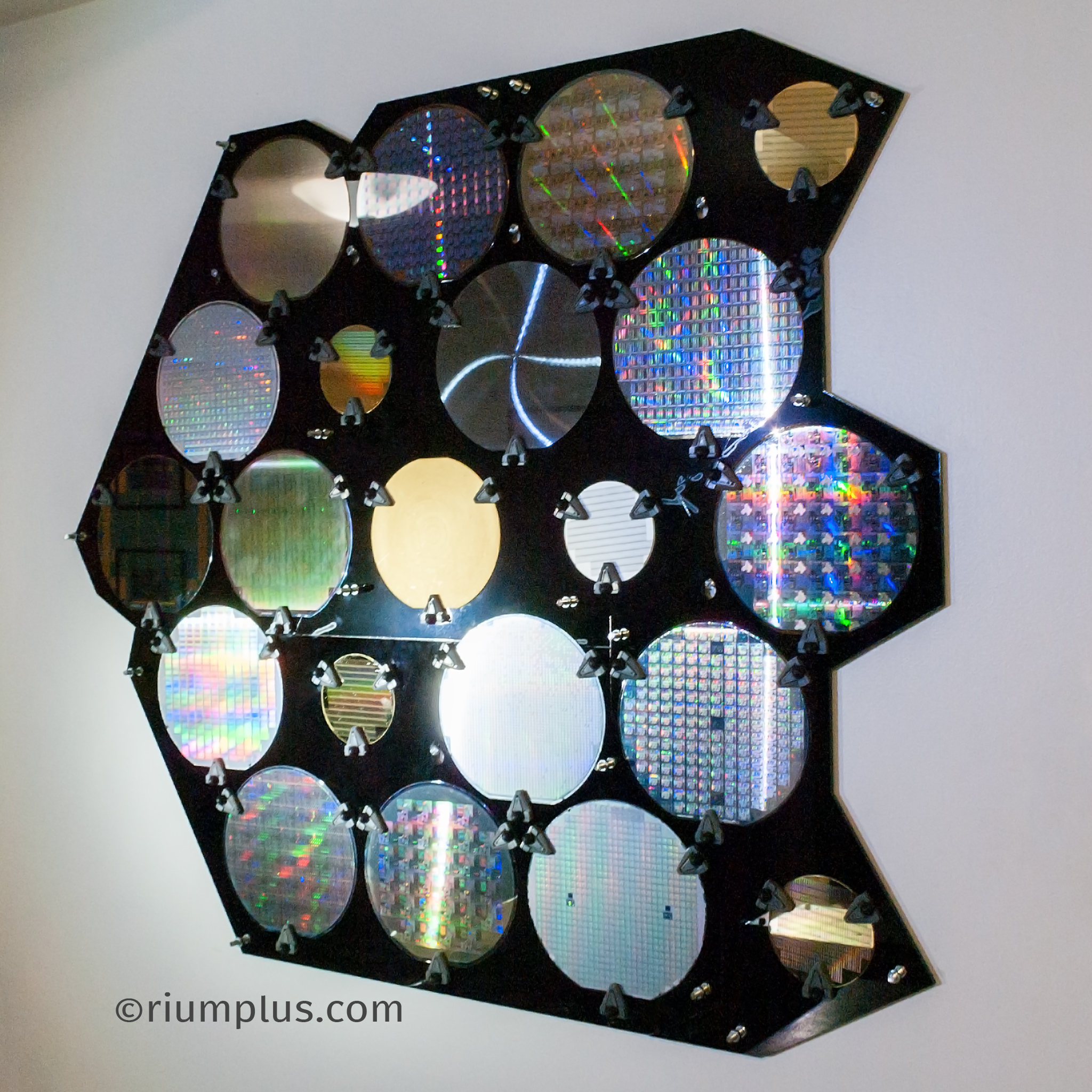
I needed some new art for one of my walls and I thought that this time I’d try making something myself. So I came up with this – an array of 21 Silicon Wafers of various types, styles and sizes. The front and back pieces are made from laser-cut acrylic, and the wafers are held in place with 3D-printed/laser-cut clips based on the Chevrons around the Stargate.
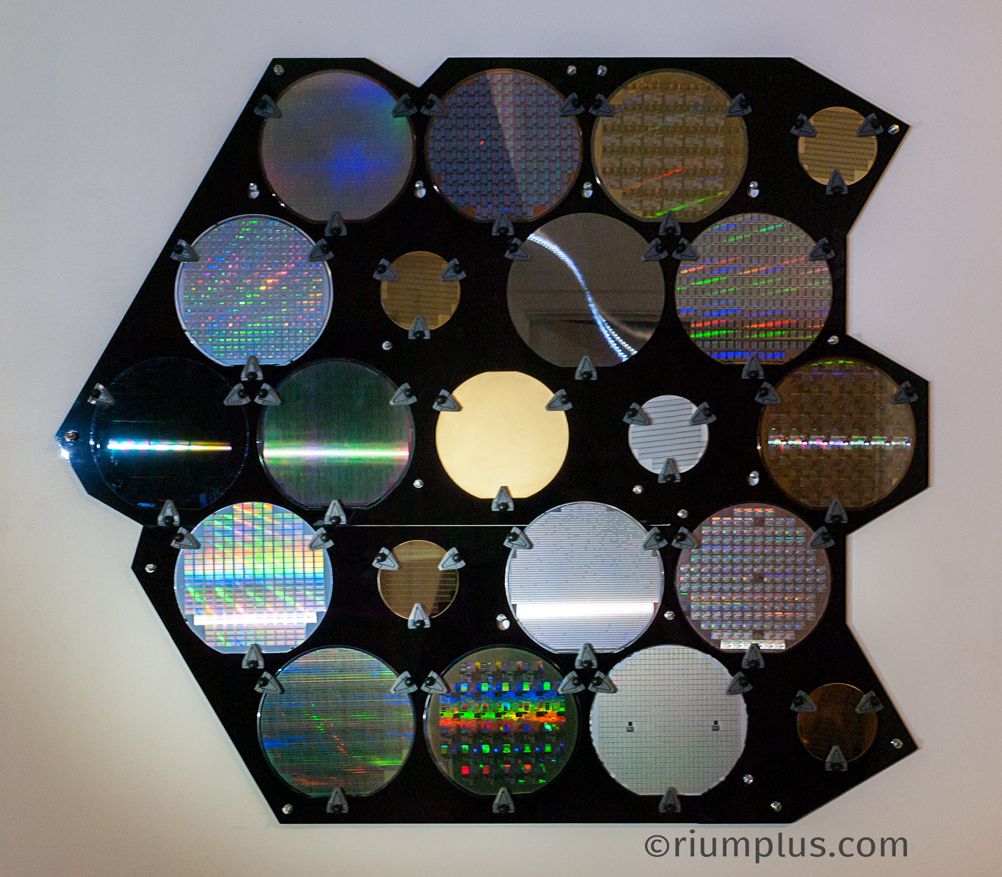
The selection of wafers is as varied as I could make it, made by multiple manufacturers across both Europe & America, from 76mm/3 inches to 150mm/6 inches in diameter, from the late 1970s though to the 2000s. Examples include an 8051-compatible microcontroller, a monitor driver chip, military/industrial grade ruggedised memory, a thermometer (DS1775), a Lexmark printer cartridge chip, an Operational Amplifier (DS4812), a MIPS R3010 floating-point co-processor similar to that used in the PlayStation 1 and the SGI workstations used to render 90s things like Jurassic Park and my favourite game Riven: The Sequel to Myst, Solar Photovoltaic panels, interposers, test patterns, bare unpolished Silicon, and even a thin layer of pure 24k gold.
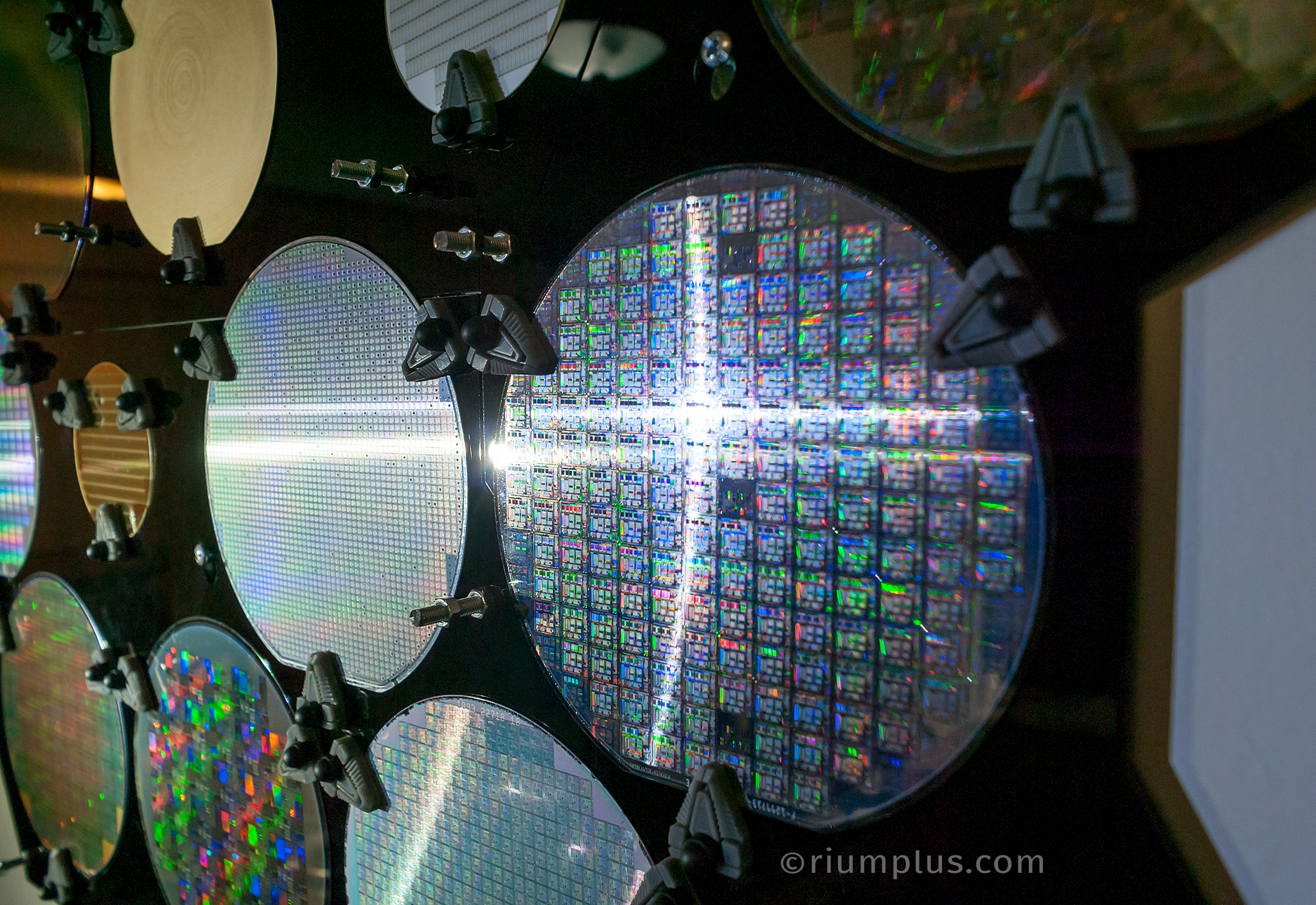
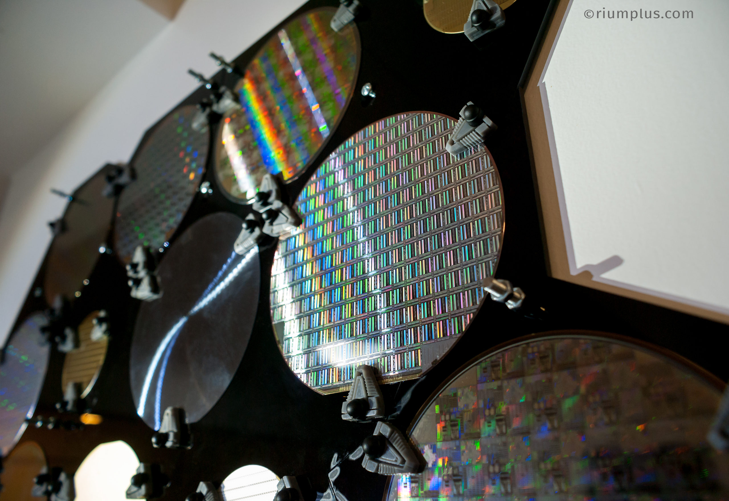
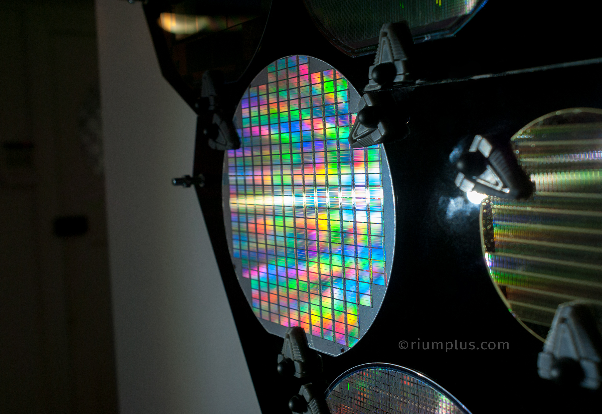
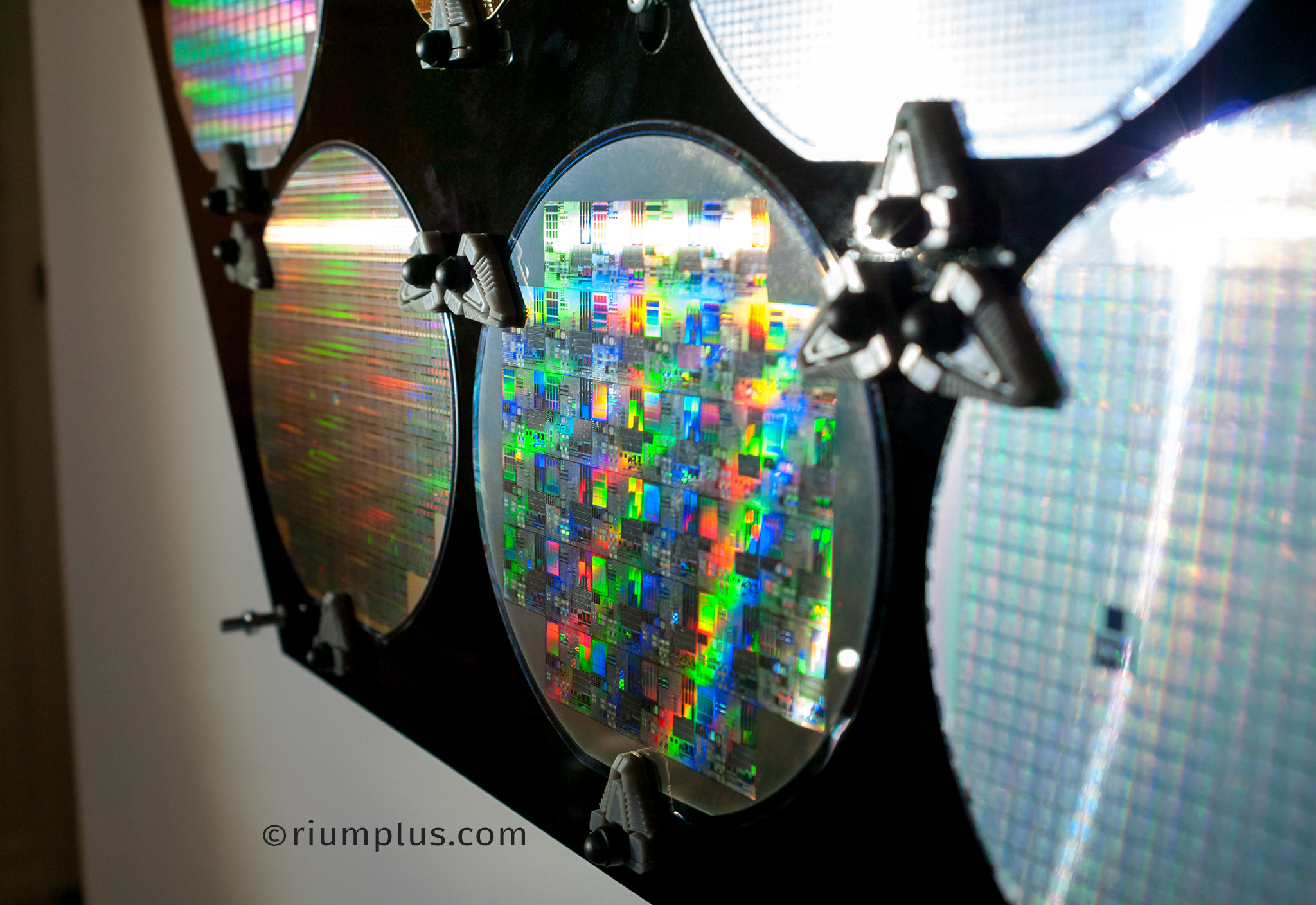
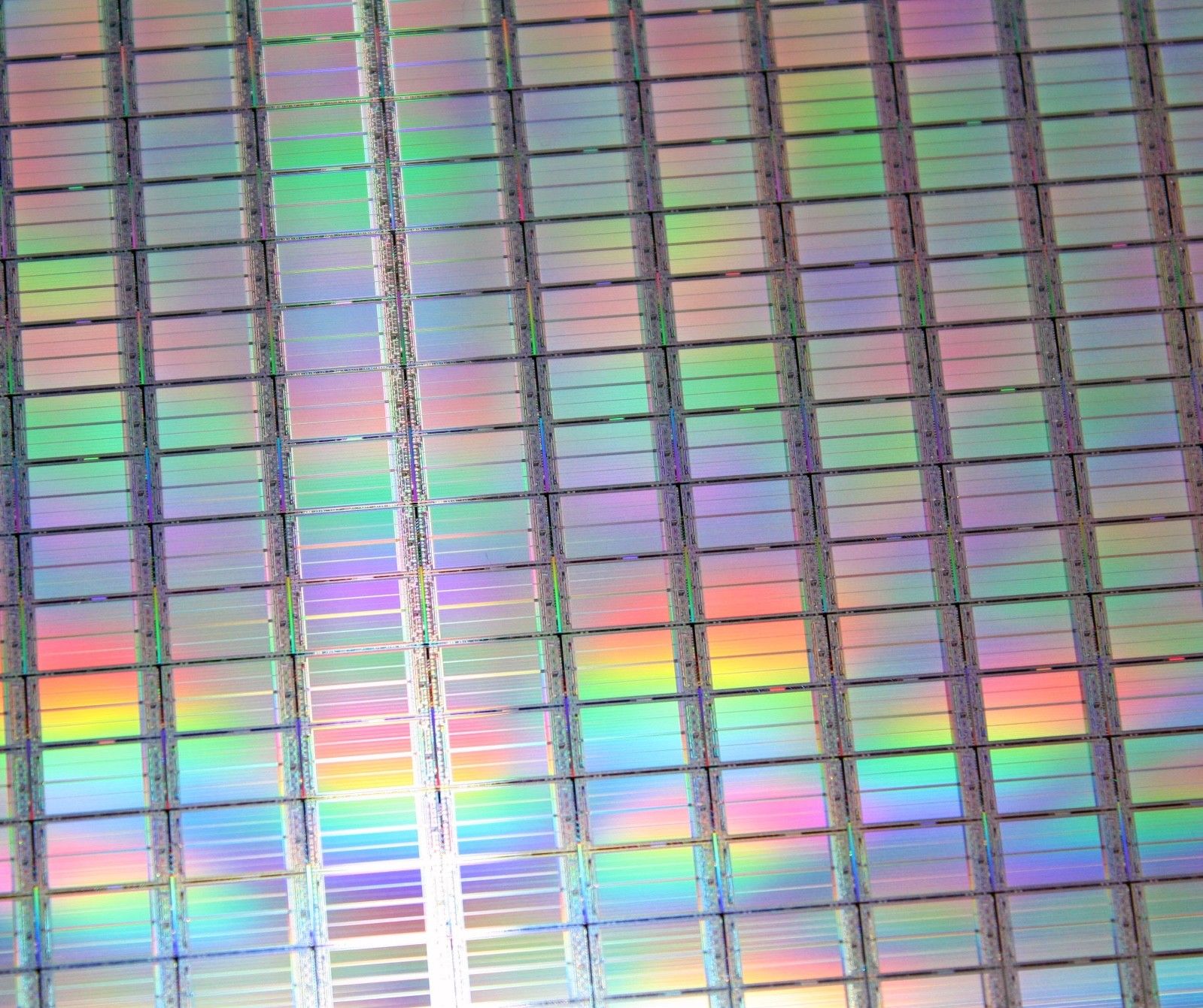
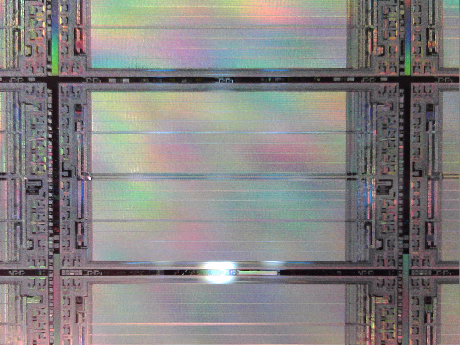
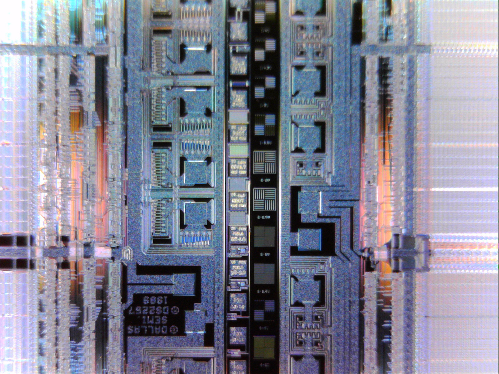
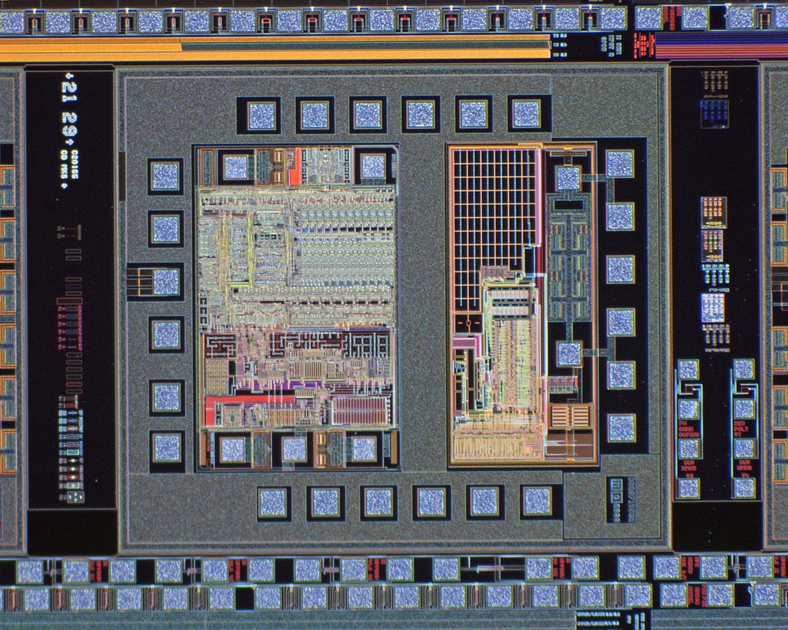
Because the etchings on the wafers are so small, a lot of them produce fantastically vibrant rainbow patterns when the light catches them at the right angle.
Some background if you don’t know what these are: computer chips are created by first growing giant cylindrical crystals of almost-pure Silicon. These are then sliced up into thin wafers and these wafers are chemically etched with all the wires & transistors using mask & a UV light source. Think of it like creating an image on photography paper using shadow puppets & a flashlight. Each wafer normally has hundreds of individual chips, or dies, etched into it. Then they’re cut up, tested, and packaged into their final form. Companies don’t normally sell the raw whole wafers but you can often buy them on eBay, mostly for older wafers and/or manufacturing runs that had defects and were destined for the bin. Prices for etched Silicon wafers vary anywhere between a few dollars to a few ten thousand dollars per wafer, depending on what it is. In total, the whole artwork is made up of many thousands of dies, far too many for me to try and count.
The first step in producing this wall artwork was to create a smaller test version, to see if the whole concept would work & how it’d look, and to iron out any kinks in the process. The prototype I created was made with just one wafer. This wafer was held in place by just the raw screw threads, which didn’t really do a good job to hold it securely in place. Valuable experience gained – come up with a better mounting system for the large design. I used a laser cutter at a lower power level to engrave-remove a few millimetres of acrylic to countersink the screw heads so they didn’t stick out. It took some trial & error but eventually I had it dialled in perfectly so the screws were perfectly flush with the acrylic. This test run was to be a present for my mother, so I picked a wafer that was made the year I was born and shines mostly pinkish (her favourite colour). The actual chips are 256K SRAM memory, so the back’s got a cheesy engraving text about “memories” on it.

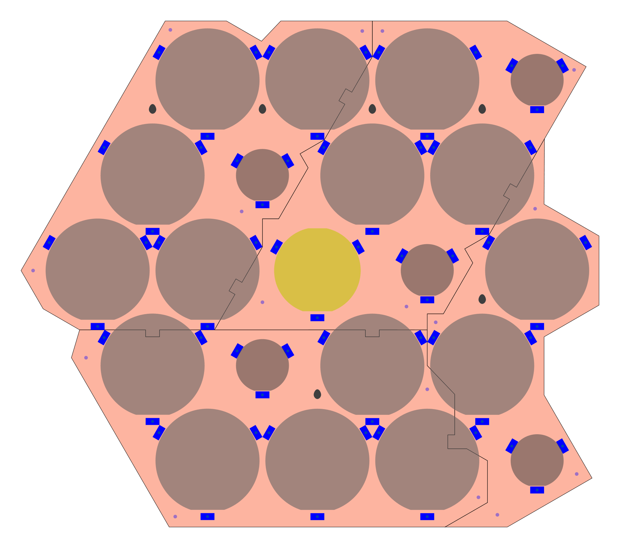
Despite some of the wafers being supposedly the same size, I noticed that a lot varied in size a little bit. To account for this, and to hold them in place so they wouldn’t rattle or rotate, each wafer was individually measured and individual mounting spacers were laser cut out of 2mm thick black backing cardboard. Since the wafers are round, I modelled the top holding clips to look like the Chevrons that surround the Stargate. These Chevron clips were 3D-printed on a resin printer – resin printers might be normally slow but when you can print 18 clips at a time, they’re not only quicker than an FDM 3D printer, the end quality is far better too.
![]()
![]()
![]()
The whole display piece was far too large (730mm high * 830mm wide) to be cut in one go on a laser cutter, so the piece was broken into 4 smaller pieces and glued together. A brutalist aesthetic was adopted for both the jigsaw-like interlocking lines as well as the whole shape. This worked well to hide some of the size limitations so I could get the maximum usable area possible out of the raw sheets of acrylic. For instance, the notch cut out on the middle left isn’t just there for aesthetics, it gives me a couple more centimetres of length for both the upper left and the bottom pieces. Without that notch, neither piece would fit within standard 300mm * 600mm sheets of Acrylic. A top layer of clear acrylic was added to both keep dust away and to protect the wafers. Some of these wafers are so delicate even a single gentle wipe with a fresh microfibre cloth will instantly destroy them (which I accidentally did trying to clean fingerprints off one, oops). It took around 9 months to build, most of which was taken up with trying to acquire as wide a variety of wafers as I could.
When doing any project involving lots of something, it’s important to remember that the time required can quickly balloon if you have to do that job many times over. For instance, there’s 63 3D-printed Chevron clips in this project – spending 8 minutes per object cleaning them up means over 8 hours just cleaning. I tried to keep the part count to a minimum, but even still there’s 21 wafers held in place by 63 3D-printed clips and 63 laser-cut mounting spacers, held together with 63 bolts plus 63 nuts and 63 black end caps, mounted on 4 sheets of black acrylic with 4 sheets of protective clear acrylic over the top, separated by 16 bolts with 48 nuts and 16 end caps… Phew. This all means the total part count for this project was 424 pieces. If I could do it again I would consider removing the laser-cut spacers and merging them with the 3D-printed Chevron clips to reduce the number of parts a little & eliminate one of the construction materials.
In the spirit of openness and encouraging others to build cool stuff too, here’s the Stargate Chevron .STL (3.0MB) and the Silicon Wafer layout .SVG. Go nuts with them!
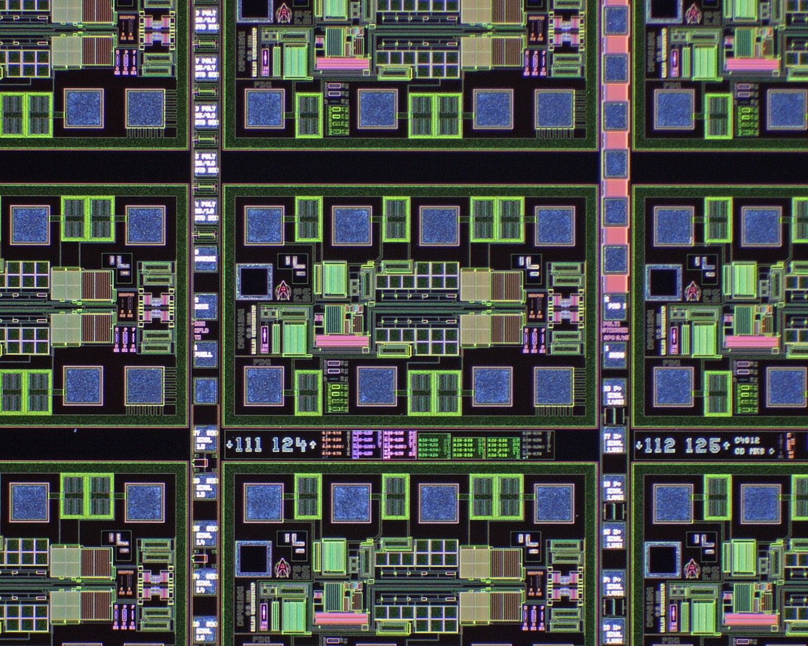
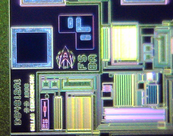
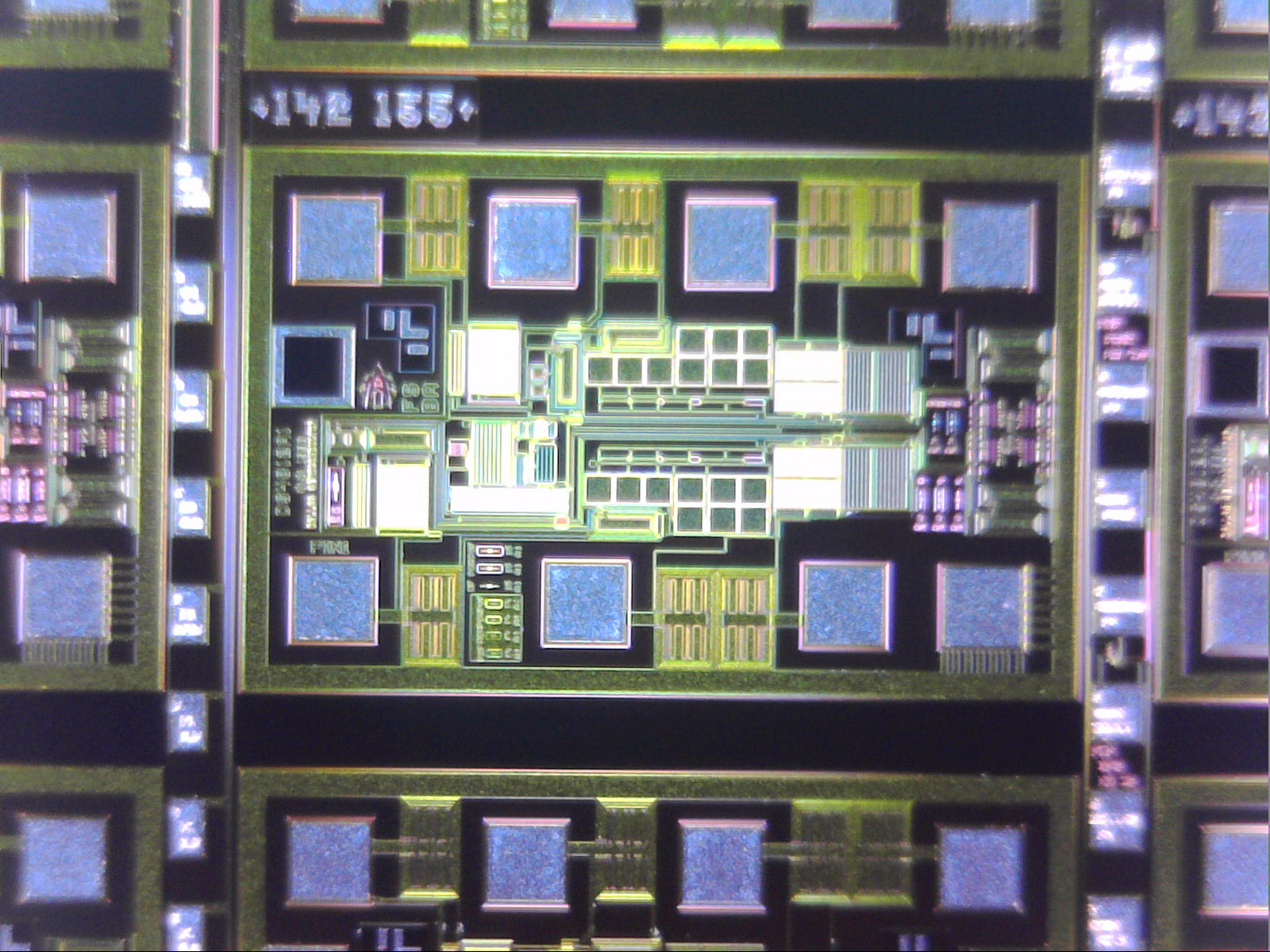
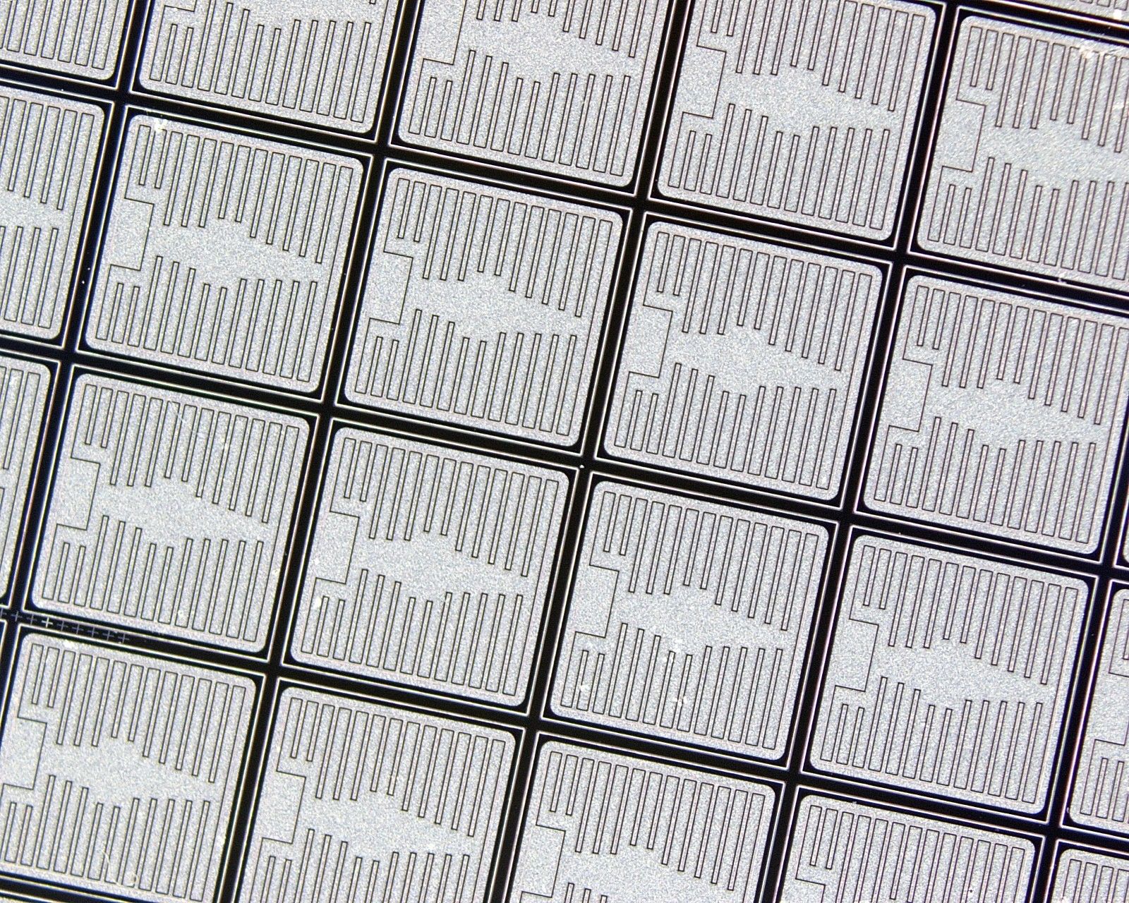
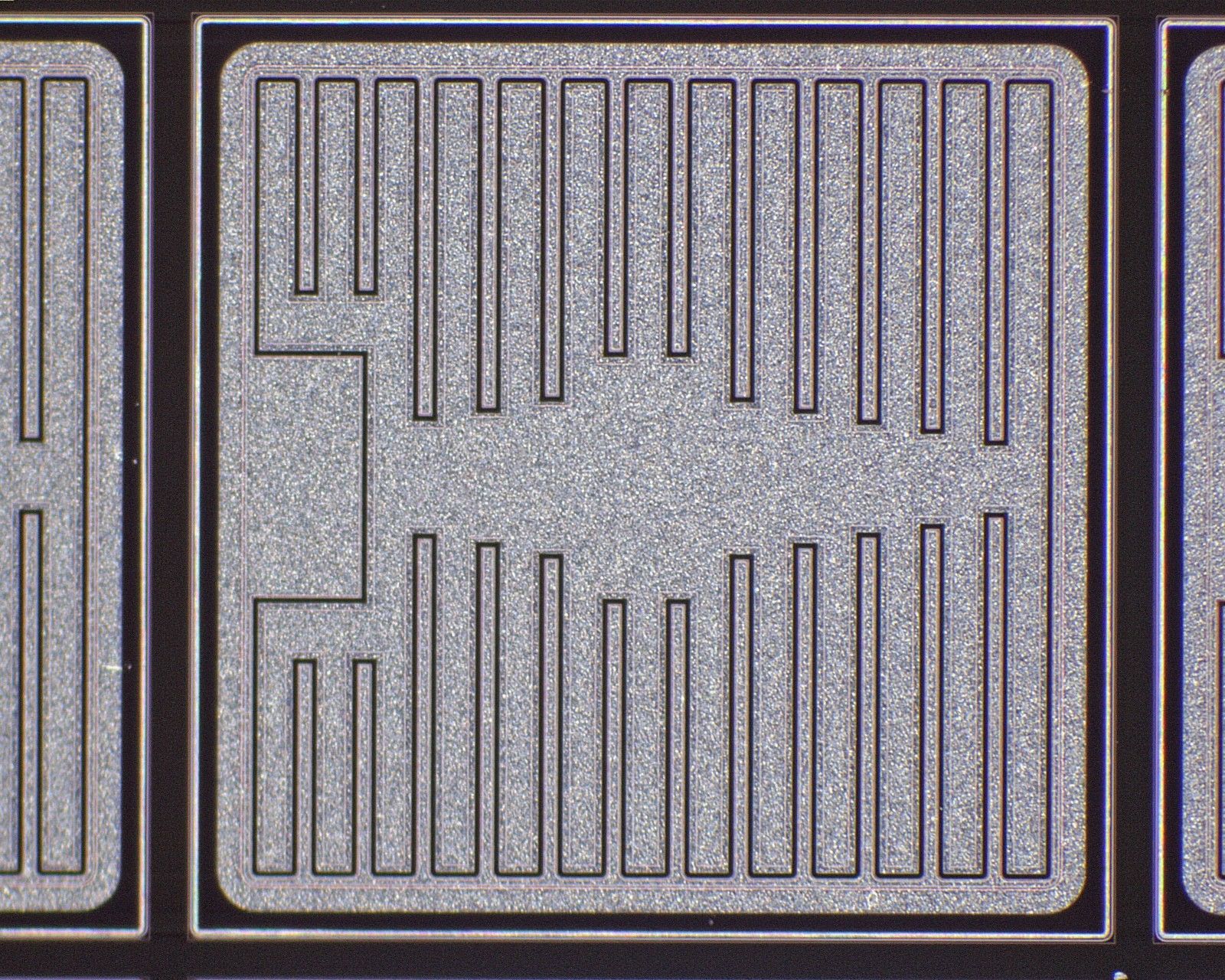
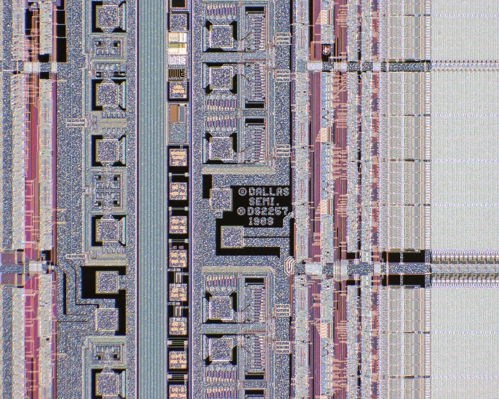
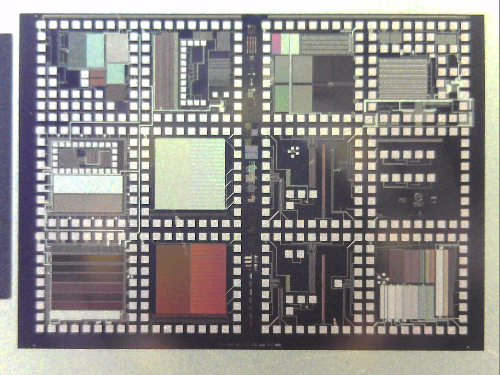
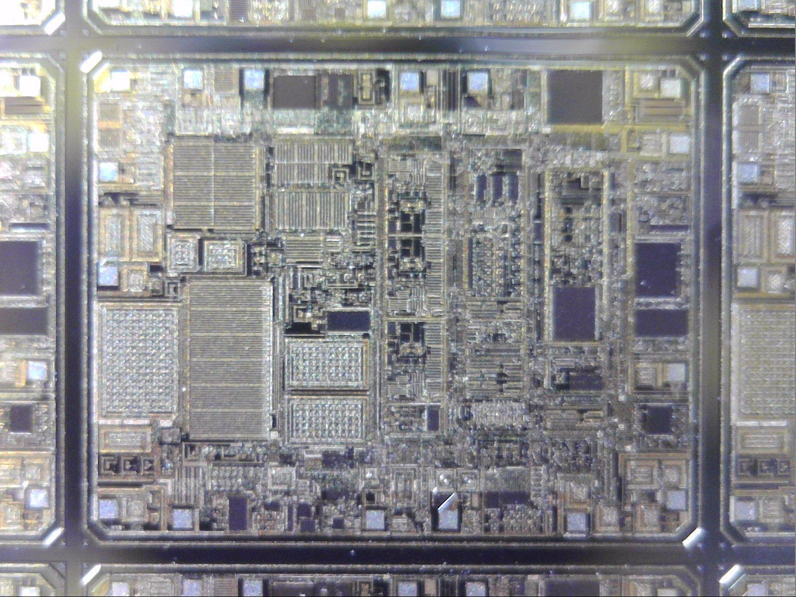
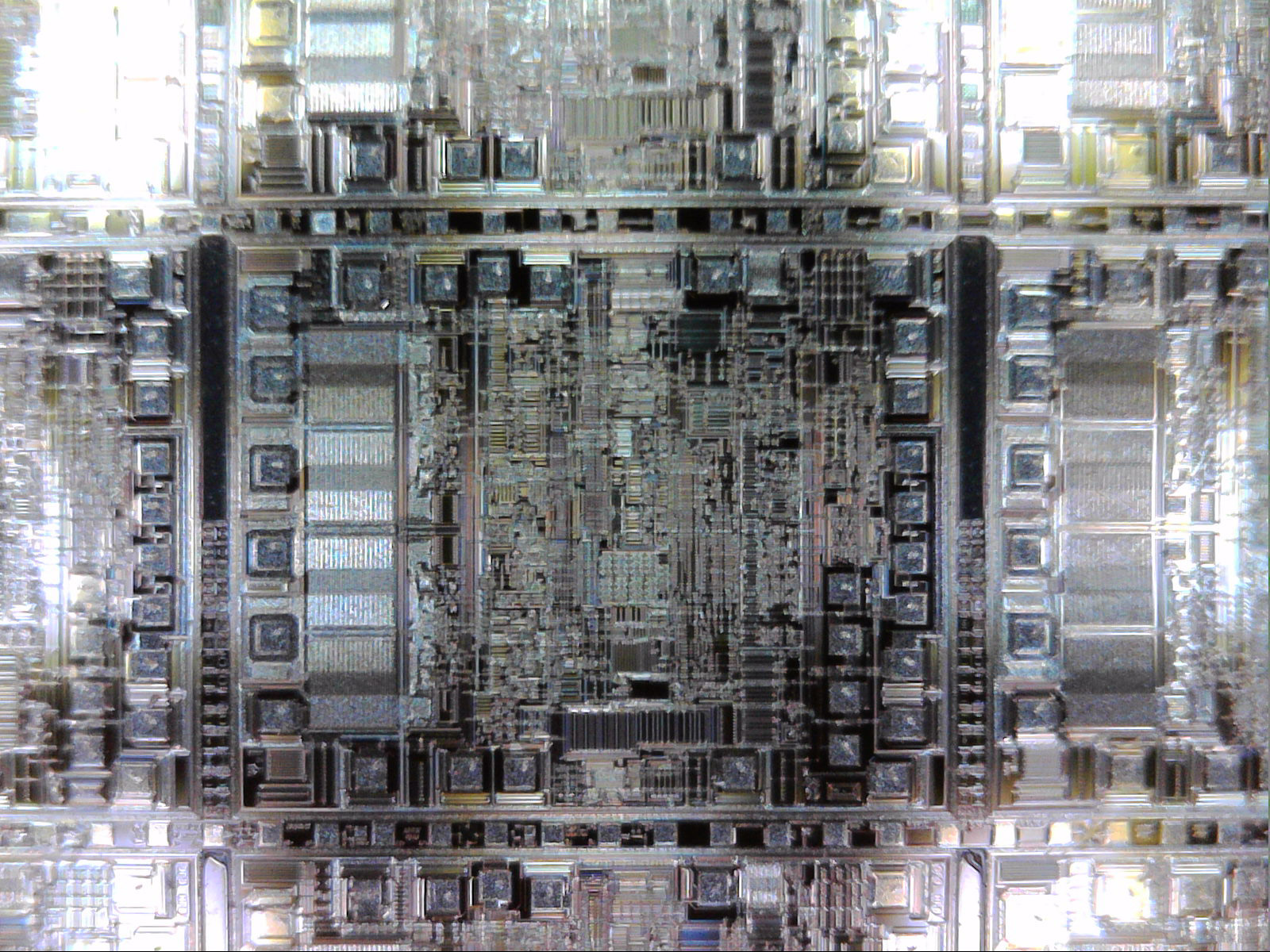
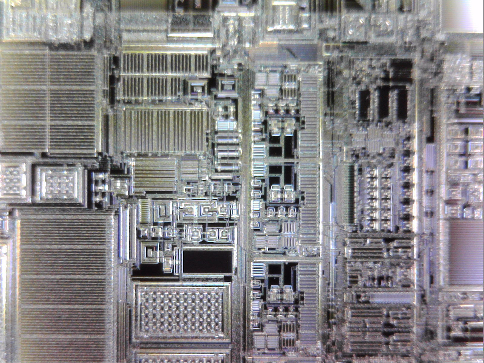
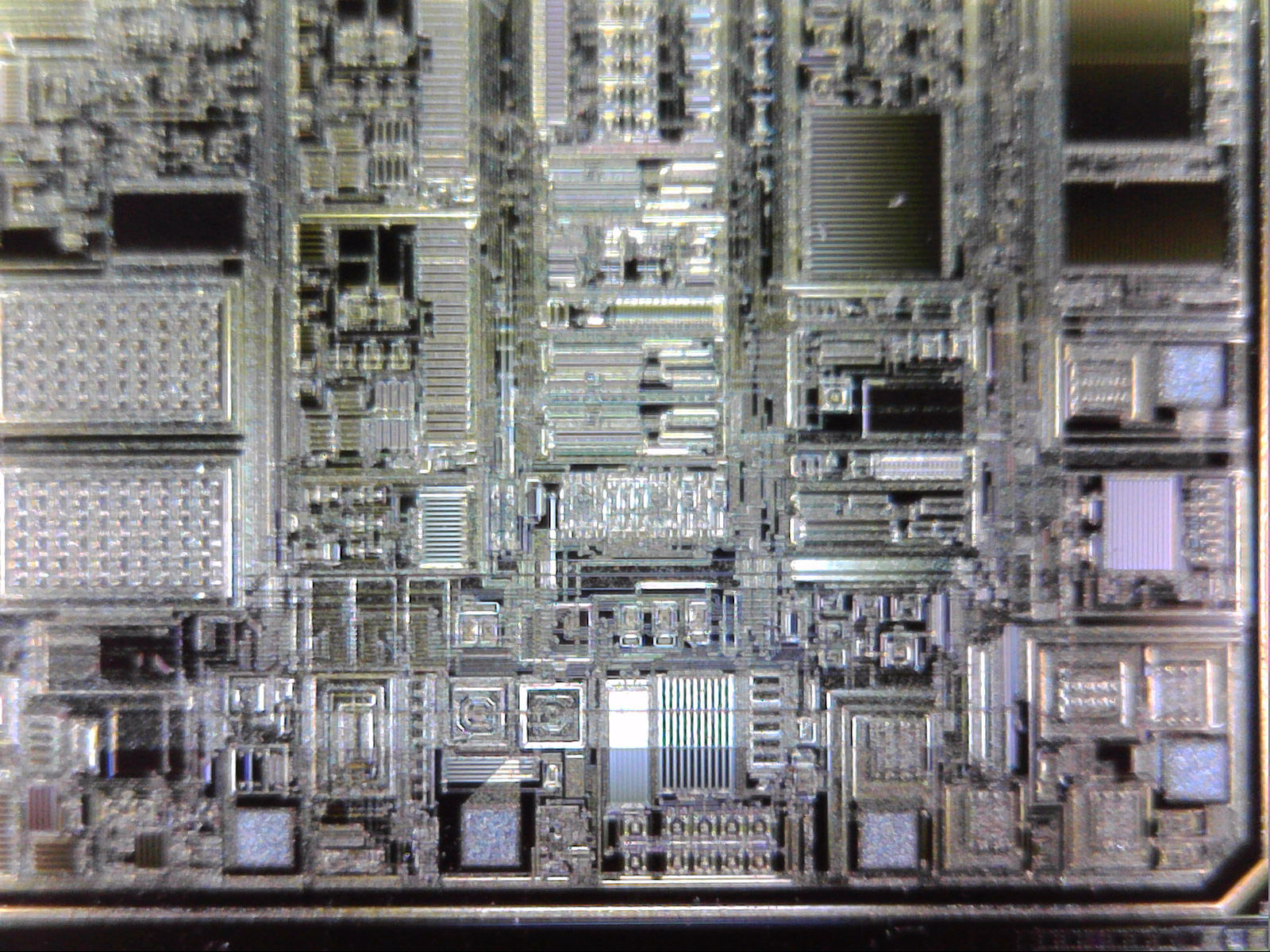
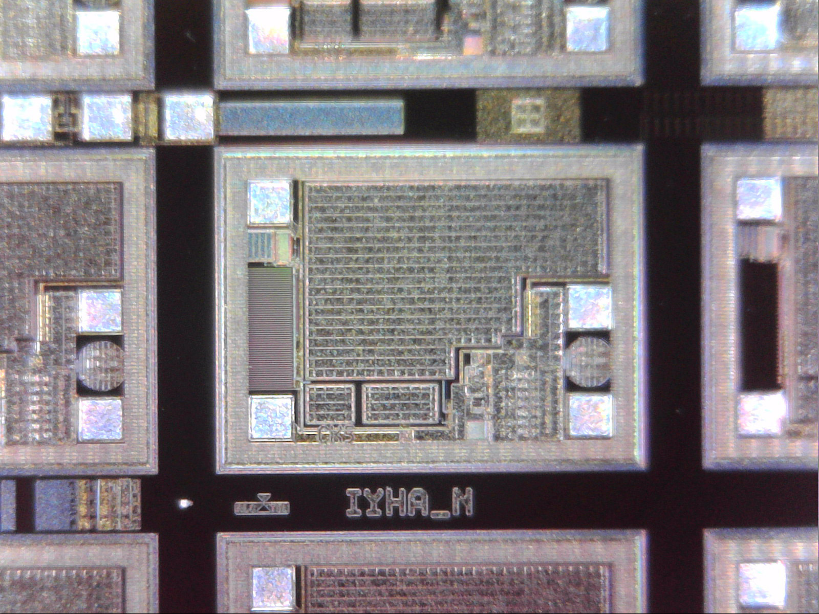
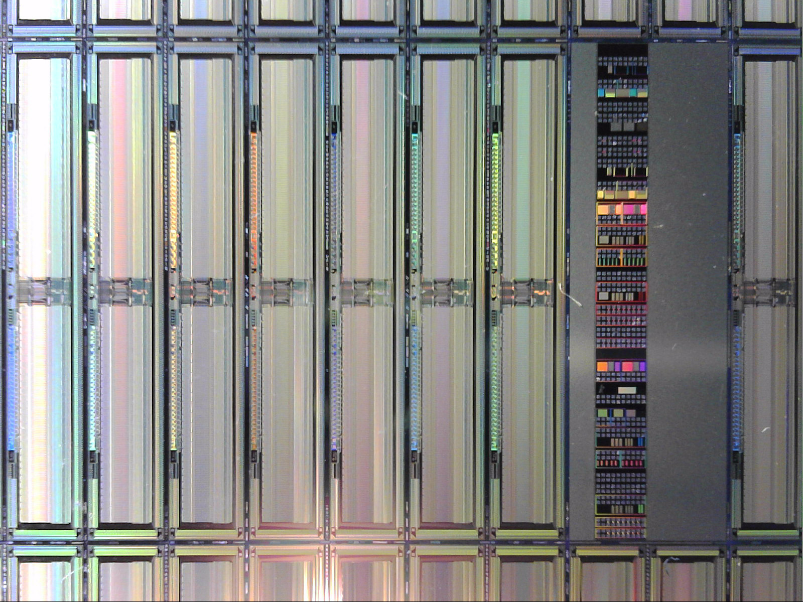
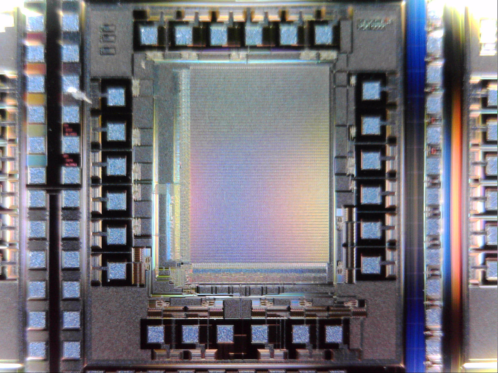
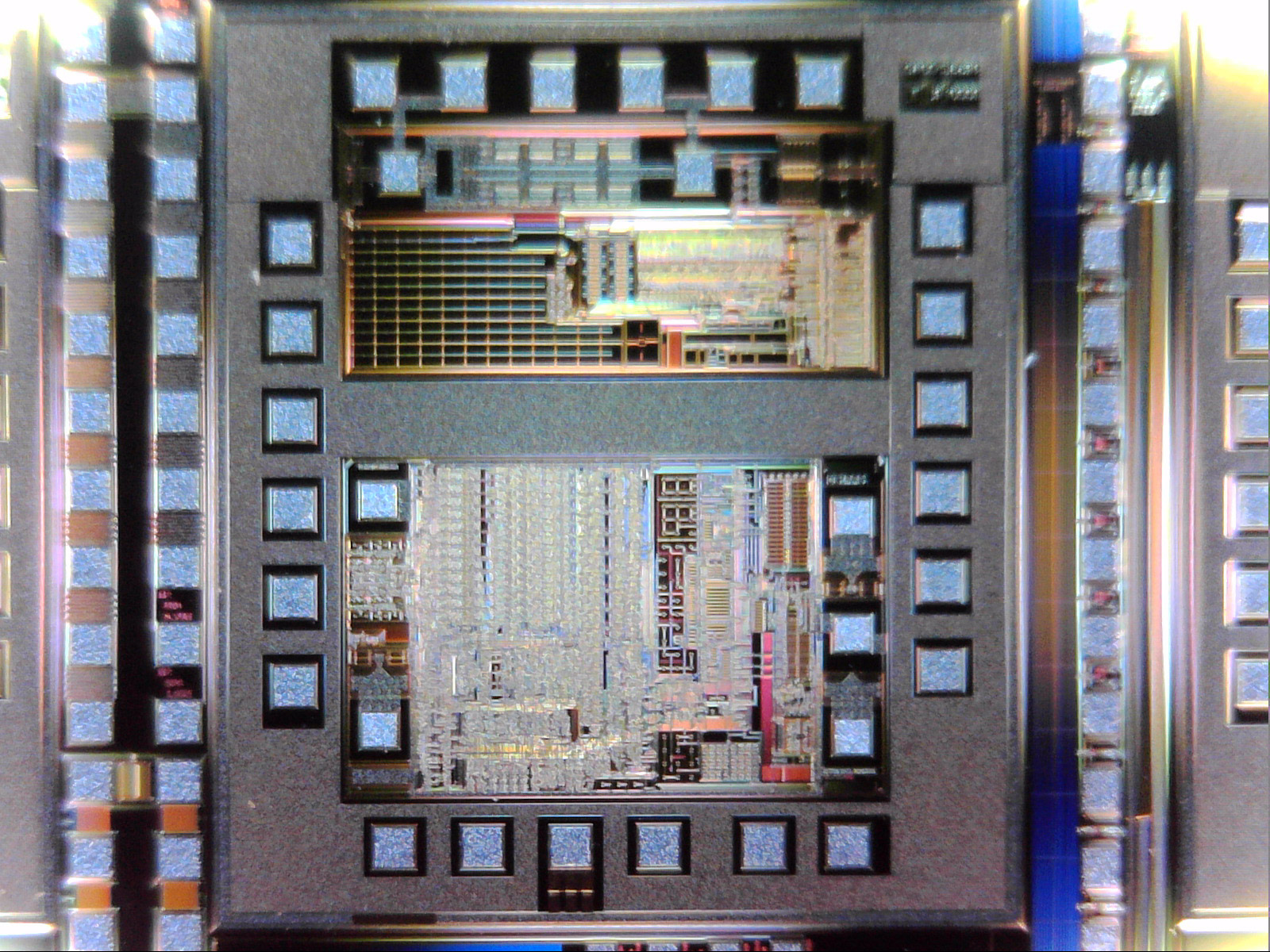
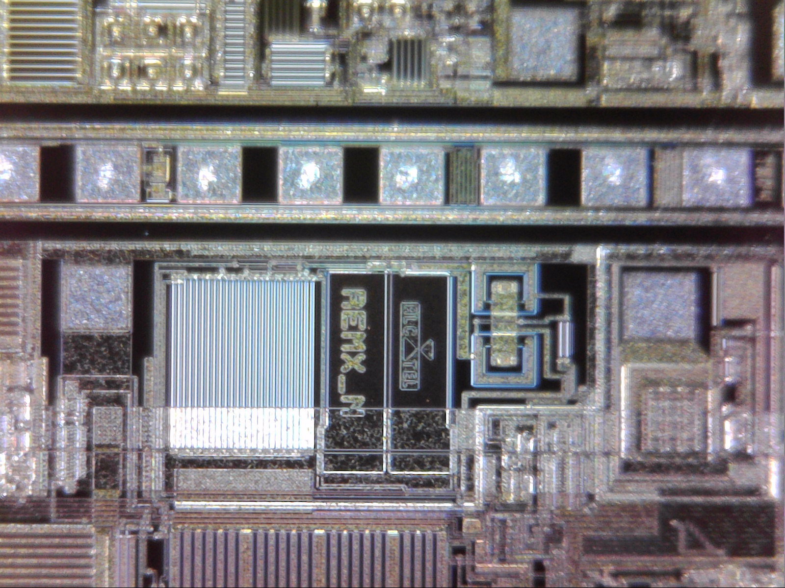
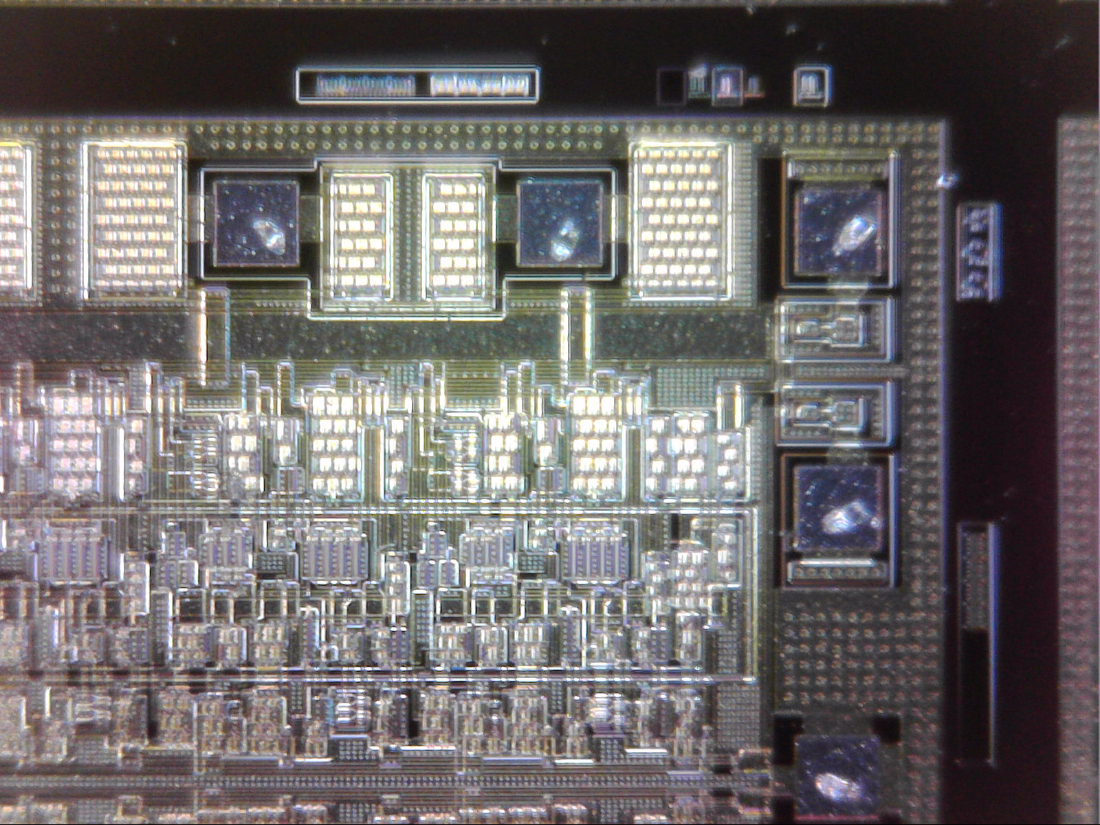
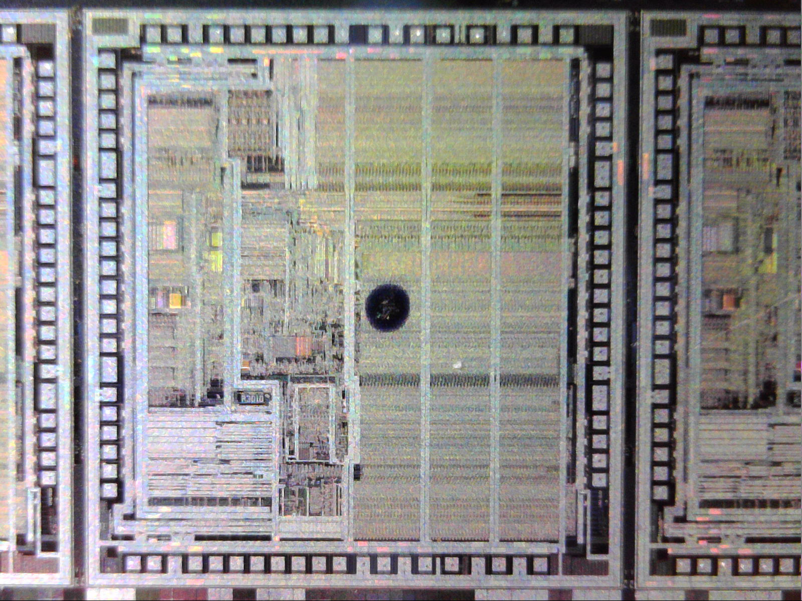
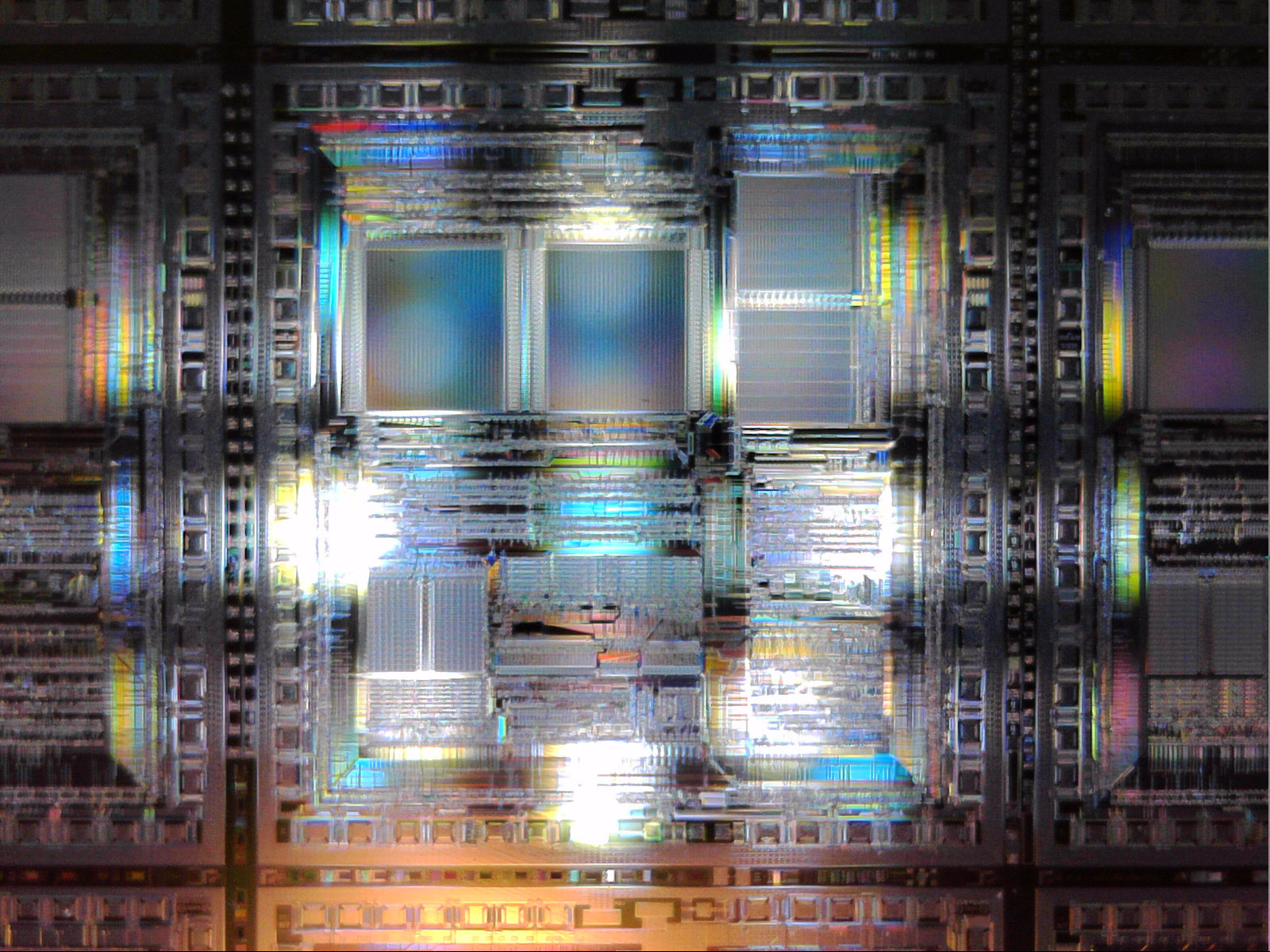
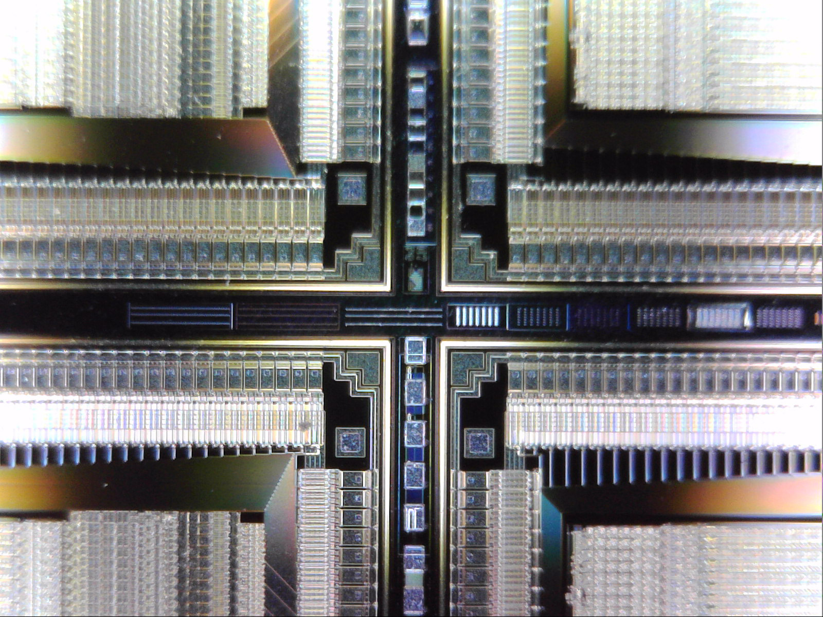
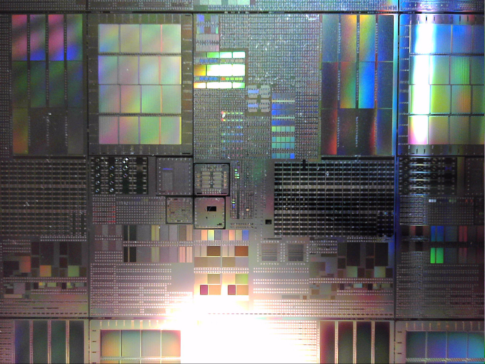
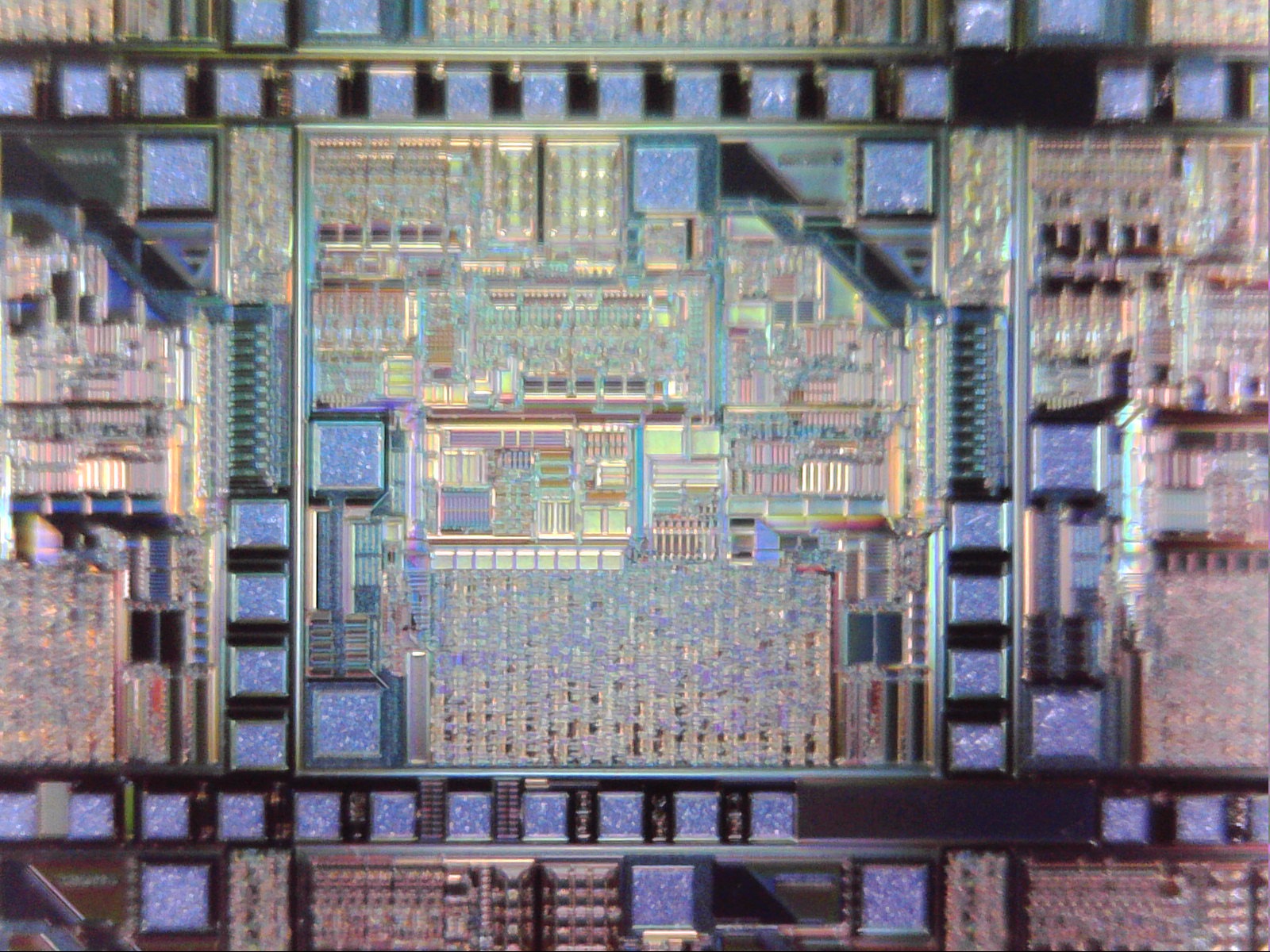
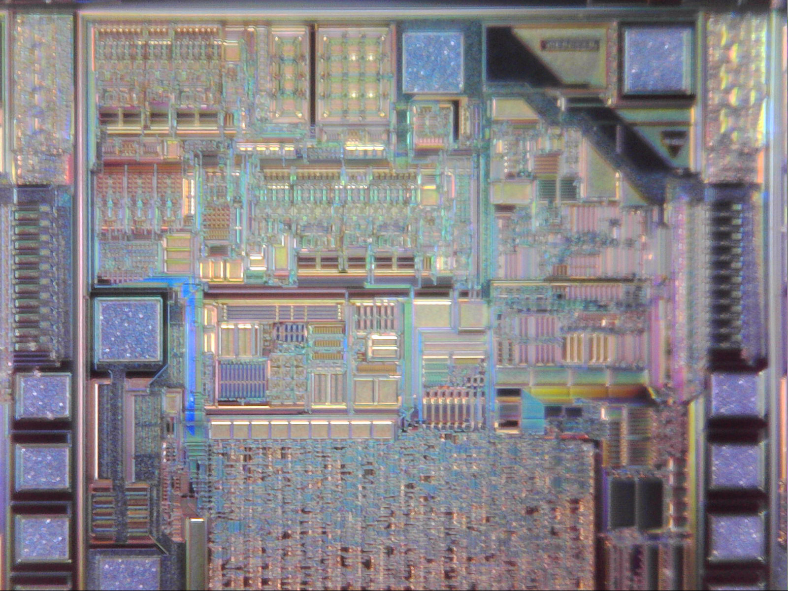
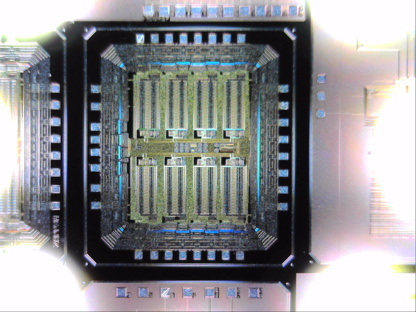
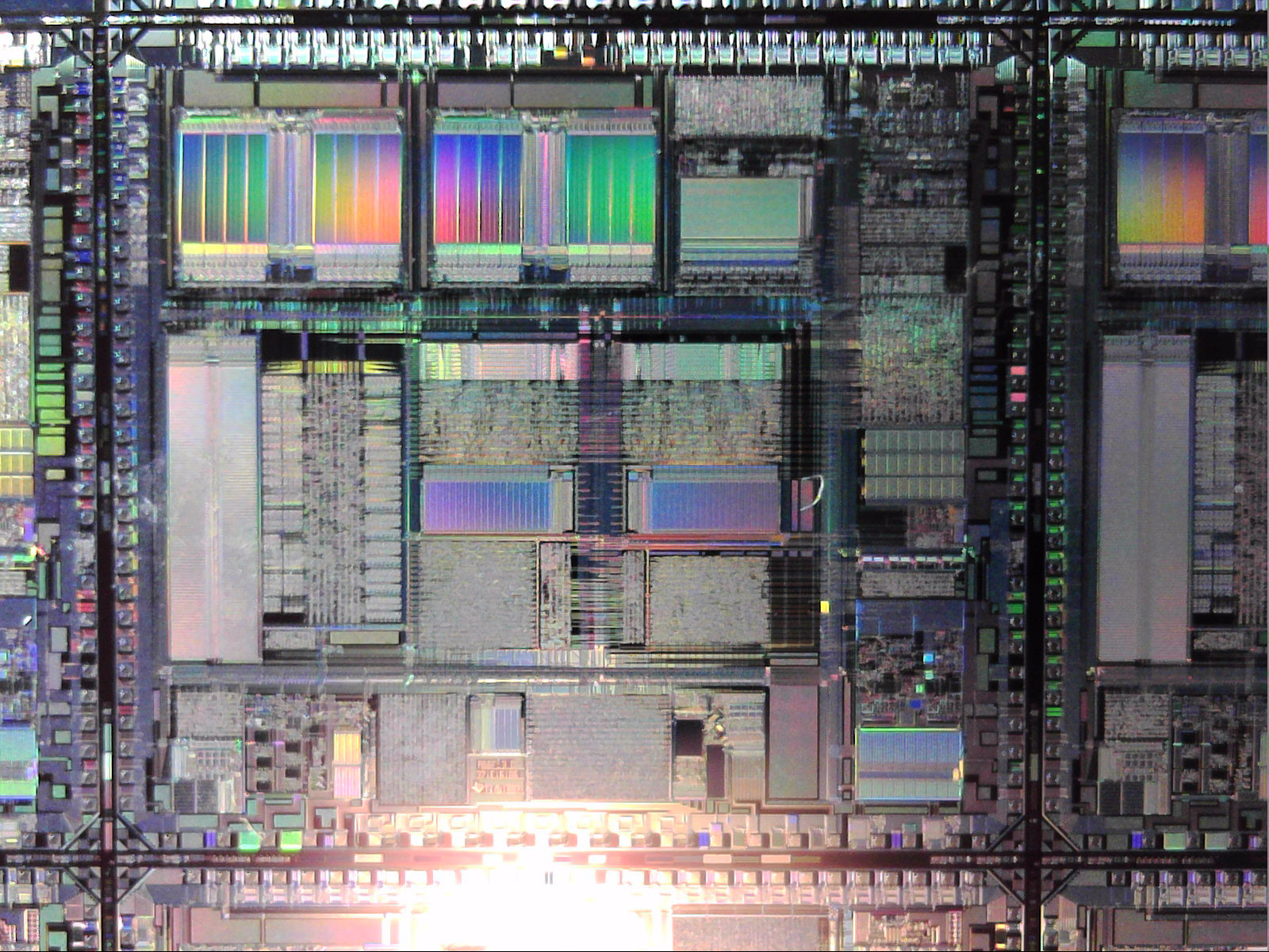
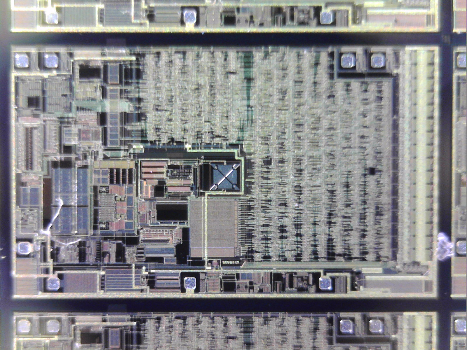
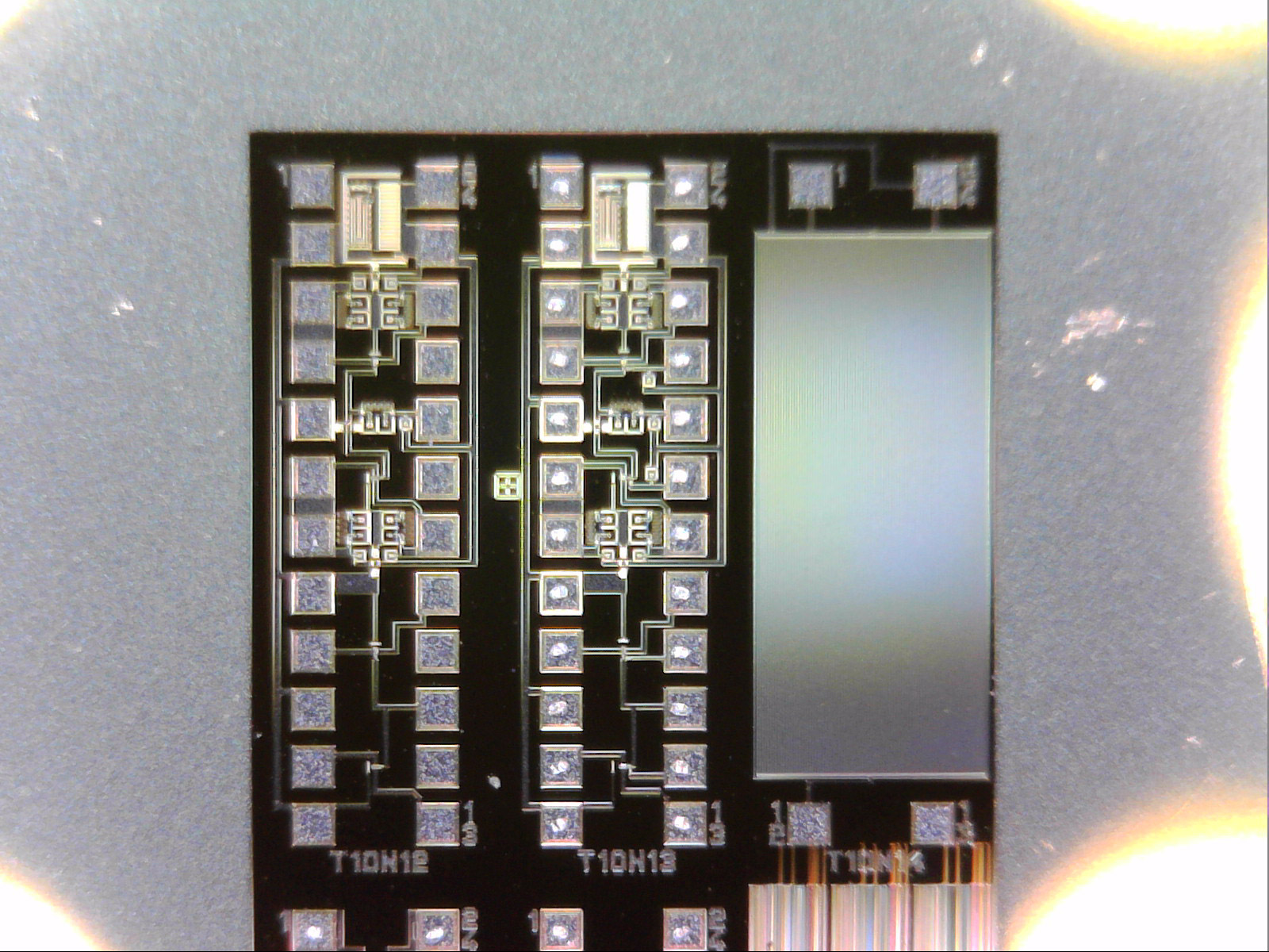
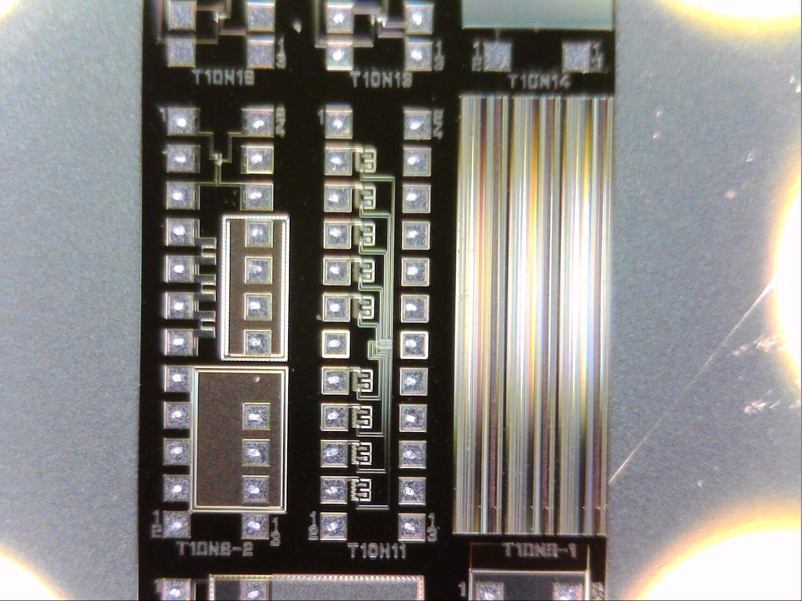
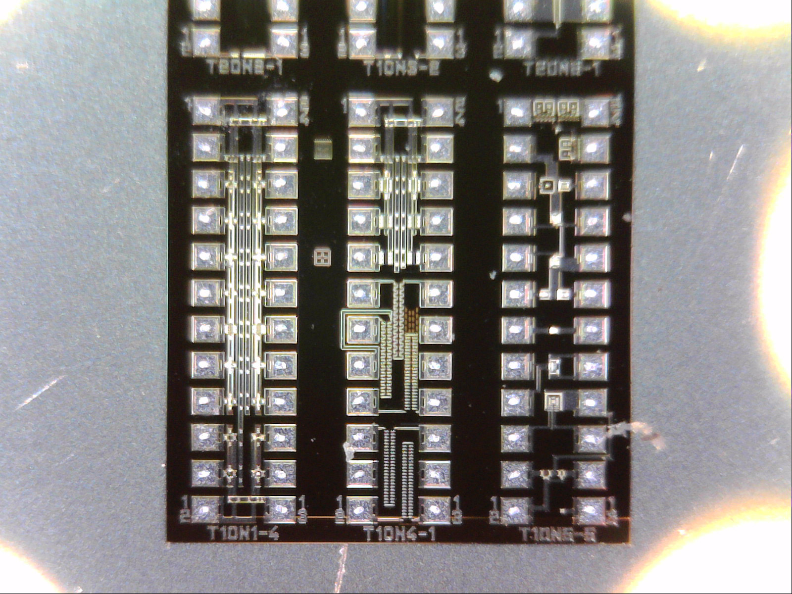
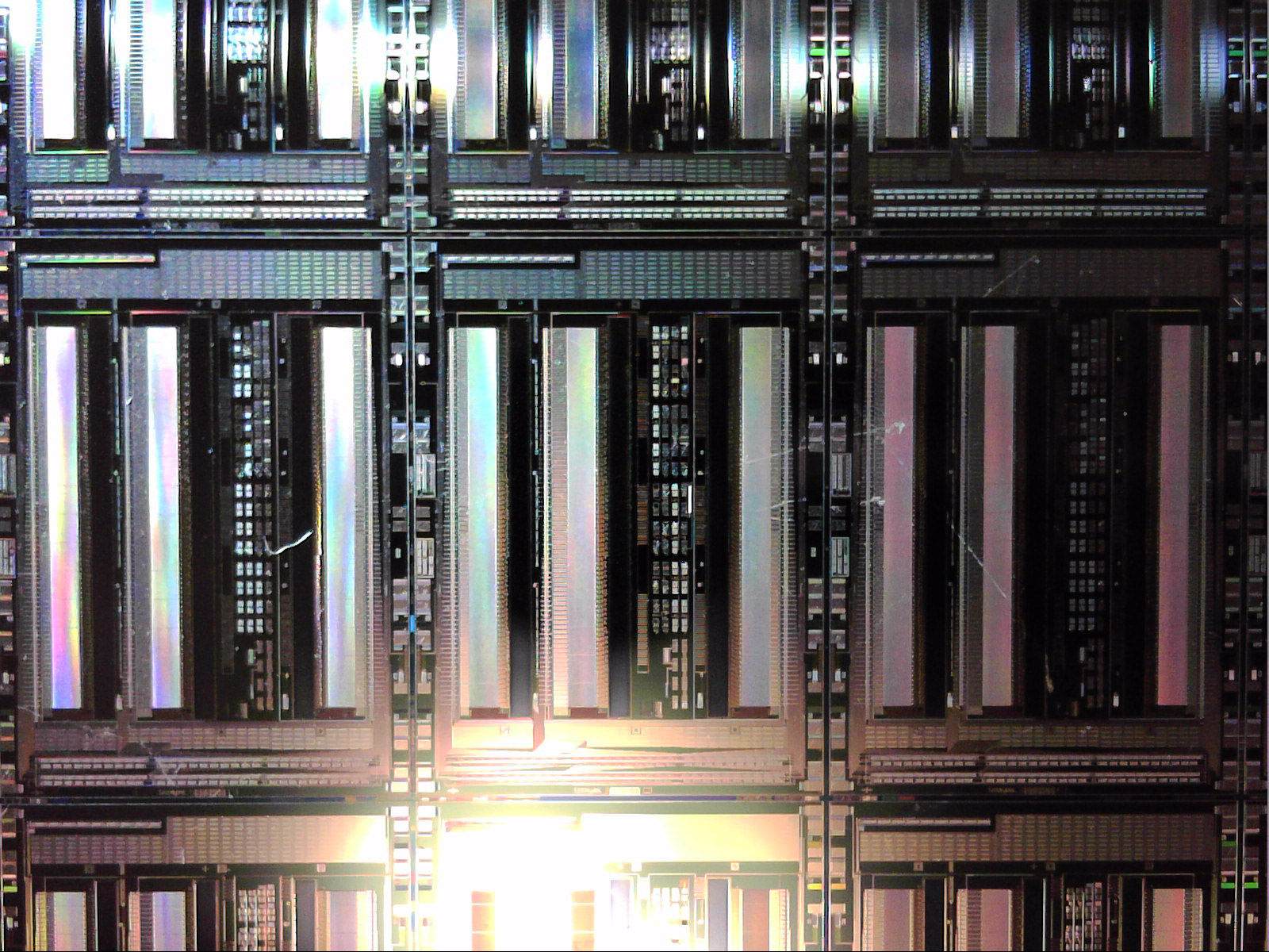
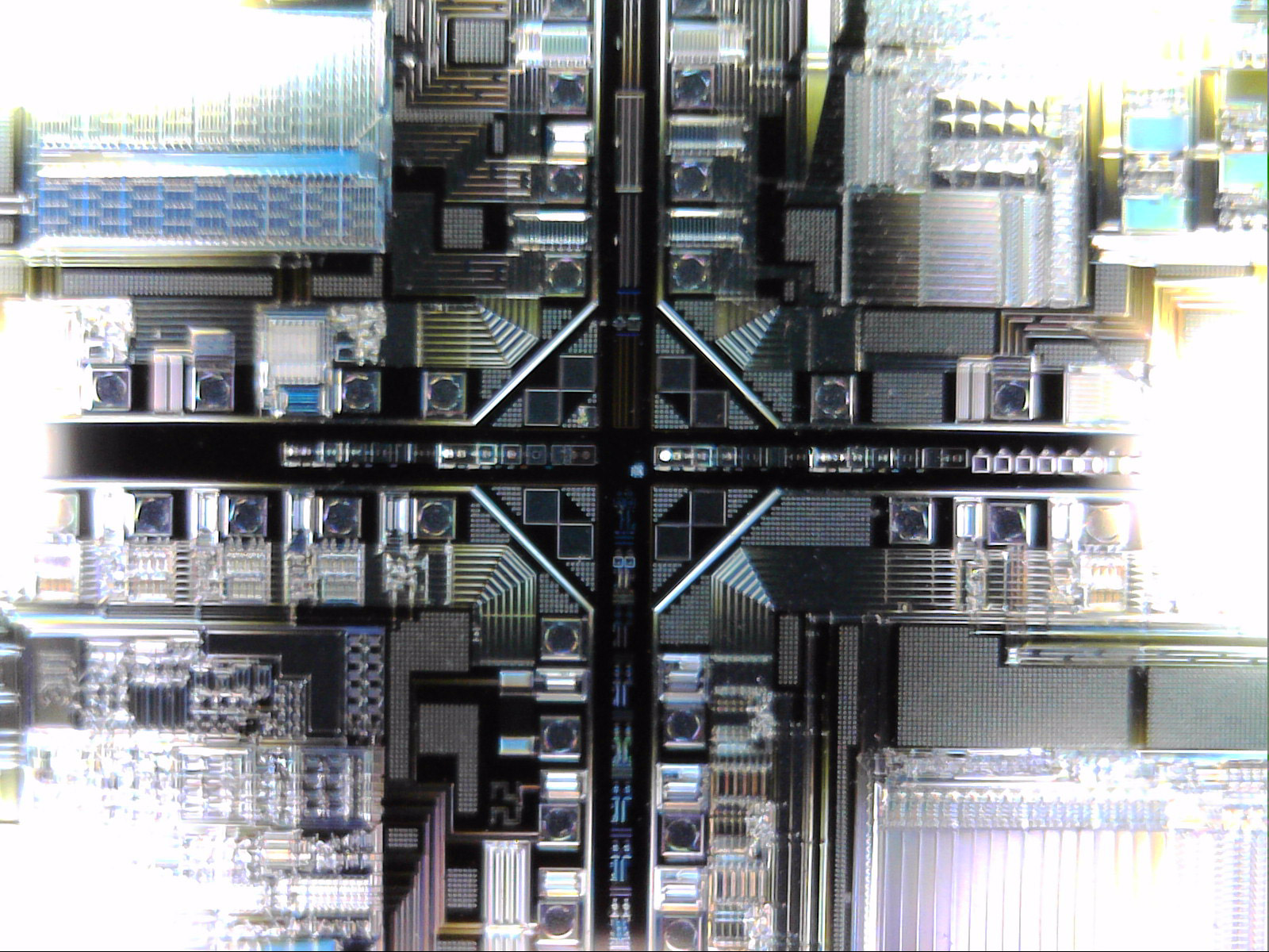
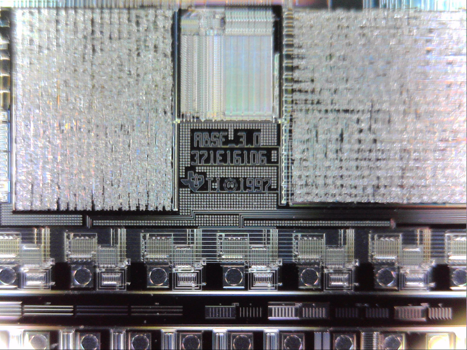
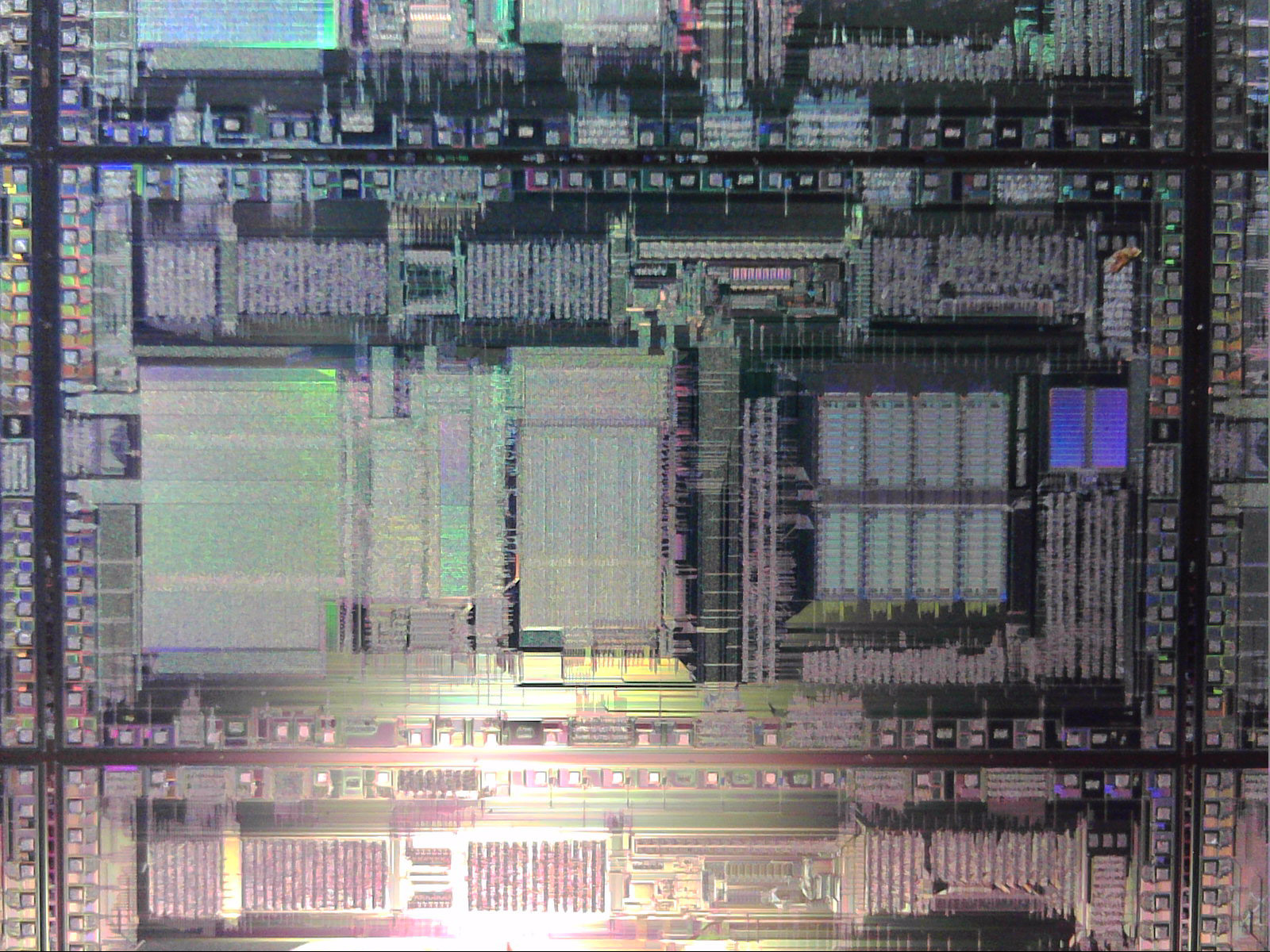
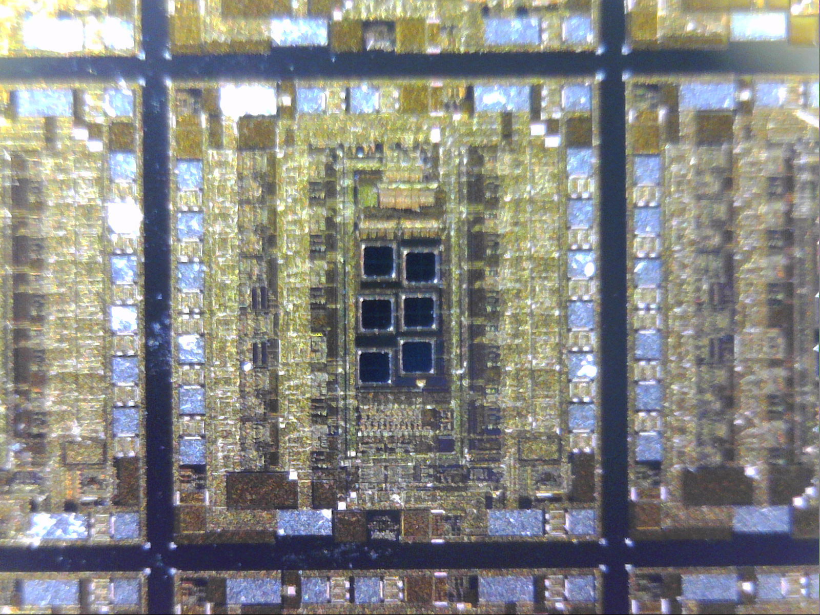
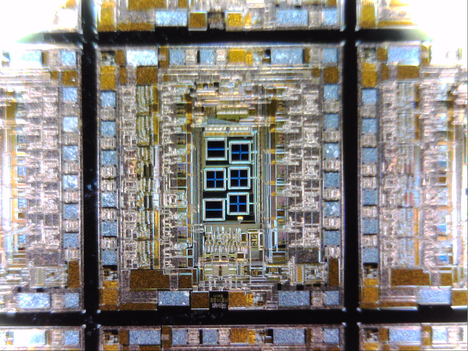
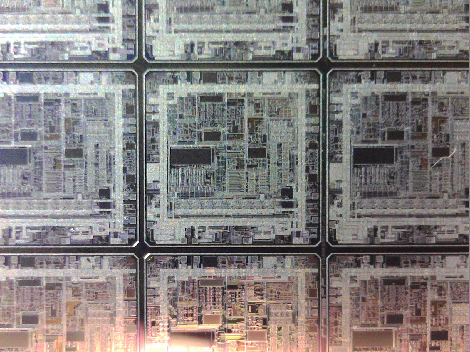
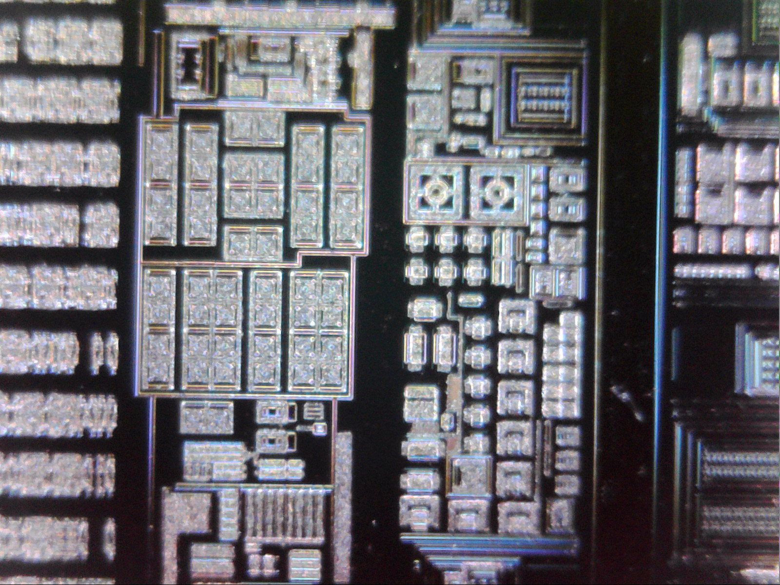
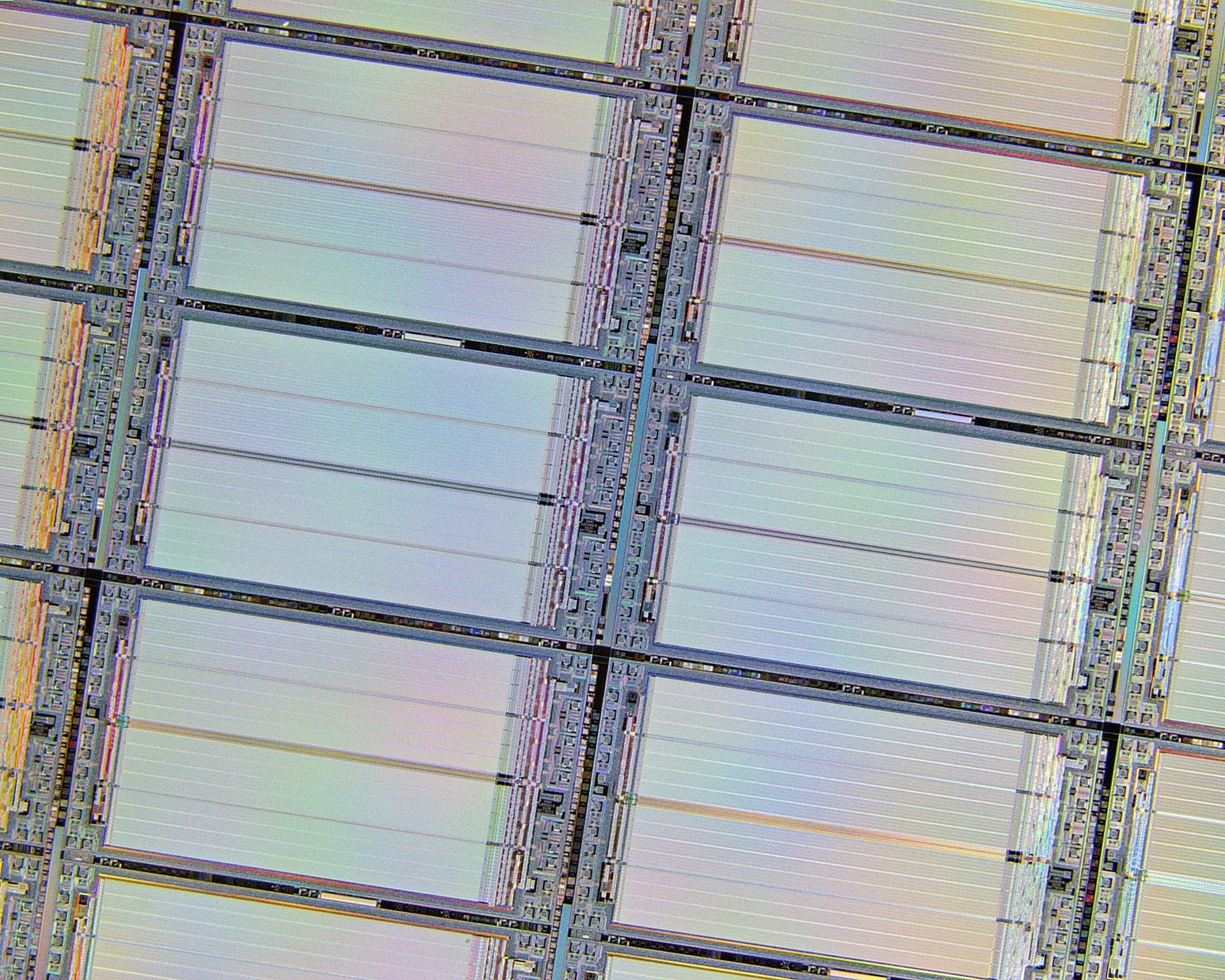
Finally, since I know some people love them, here’s some photos of the Silicon Wafers taken with a 500x digital microscope so you can see what they look like up close. The patterns vary widely depending on the wafer – memory tends to look like repeating structures, logic gates tend to look like a random mess, and sensors/anything analogue/test patterns tend to look like some abstract painting. I could swear that one of them has Silicon art of an OR-gate with one leg shorter to make it look more like the Star Trek logo, but it’s just slightly beyond the magnification limits of my microscope so I can’t photograph it. Most of these are from the wafers you see in this artwork, but there’s a few from other wafers I didn’t use.
Similar Posts

Gradientment, the Image Gradient Map Generator
Gradientment converts your 2D images into two overlapping 1D gradients & spits out the highly-compacted CSS used to generate these gradient maps, for perceived-faster progressive image loading or for artistic purposes. Sure, you could use...
New Andotrope Website
This is just a quick update to say that I’ve launched a new website for my Andotrope omnidirectional displays! Having a dedicated space to promote them makes it easier to share them with others. Plus,...
There are no comments yet, add one below.
Leave a Reply